Invented by Matthew H. Frey, Ta-Hua Yu, Kari A. McGee, Hui Luo, William B. Kolb, Brant U. Kolb, Moses M. David, Lijun Zu, 3M Innovative Properties Co
Patterned substrates with darkened conductor traces are highly sought after due to their unique features and benefits. The darkened conductor traces provide improved visibility and contrast, making it easier for engineers and technicians to identify and troubleshoot any potential issues. This is particularly important in complex electronic systems where multiple components and traces are densely packed together.
Moreover, the darkened conductor traces offer enhanced heat dissipation capabilities. As electronic devices become smaller and more powerful, heat management becomes a critical concern. The darkened traces help to dissipate heat more efficiently, preventing overheating and ensuring optimal performance.
Another advantage of patterned substrates with darkened conductor traces is their aesthetic appeal. These substrates are often used in consumer electronics, where design and appearance are essential factors. The darkened traces create a sleek and modern look, enhancing the overall visual appeal of the device.
The market for patterned substrates with darkened conductor traces is driven by various industries. The automotive sector, for instance, relies heavily on PCBs with darkened traces for advanced driver-assistance systems (ADAS) and infotainment systems. These systems require high-speed data transmission and reliable connectivity, which can be achieved through the use of patterned substrates with darkened conductor traces.
The telecommunications industry is another major contributor to the market. With the increasing demand for faster and more reliable communication networks, PCBs with darkened traces are used in networking equipment, routers, and switches. The darkened traces ensure signal integrity and minimize signal loss, resulting in improved network performance.
Furthermore, the healthcare sector is adopting patterned substrates with darkened conductor traces for medical devices and equipment. These substrates are used in devices such as pacemakers, defibrillators, and medical imaging systems. The darkened traces provide better visibility during surgical procedures and diagnostics, enabling healthcare professionals to make accurate and timely decisions.
In terms of geographical distribution, the market for patterned substrates with darkened conductor traces is witnessing significant growth in Asia-Pacific. The region is home to several leading electronics manufacturers, and the increasing demand for consumer electronics and automotive products is driving the market. North America and Europe also contribute to the market growth, with a focus on advanced technologies and high-end applications.
In conclusion, the market for patterned substrates with darkened conductor traces is expanding rapidly, driven by the need for improved visibility, heat dissipation, and aesthetic appeal. Industries such as automotive, telecommunications, and healthcare are the major contributors to this market. As technology continues to advance, the demand for patterned substrates with darkened conductor traces is expected to grow further, providing opportunities for manufacturers and suppliers in the electronics industry.


The 3M Innovative Properties Co invention works as follows
The present disclosure discloses an article with a substrate that has a first nanostructured side and a second opposing surface, and a conductor pattern disposed on the surface of the first surface. This conductor pattern is formed by multiple traces. The micropattern can have an open-area fraction of greater than 80%. The conductor micropattern traces may have less than 50% specular reflectance when viewed in a plane orthogonal and towards the first surface. The nanostructured surfaces may have nanofeatures with a height of 50-750 nanometers and a width between 15-200 nanometers. These articles can be used in displays for hand-held devices, computers, and tablets. “They are also used in antennas as well as EMI shields.


Background for Patterned Substrates with Darkened Conductor Traces
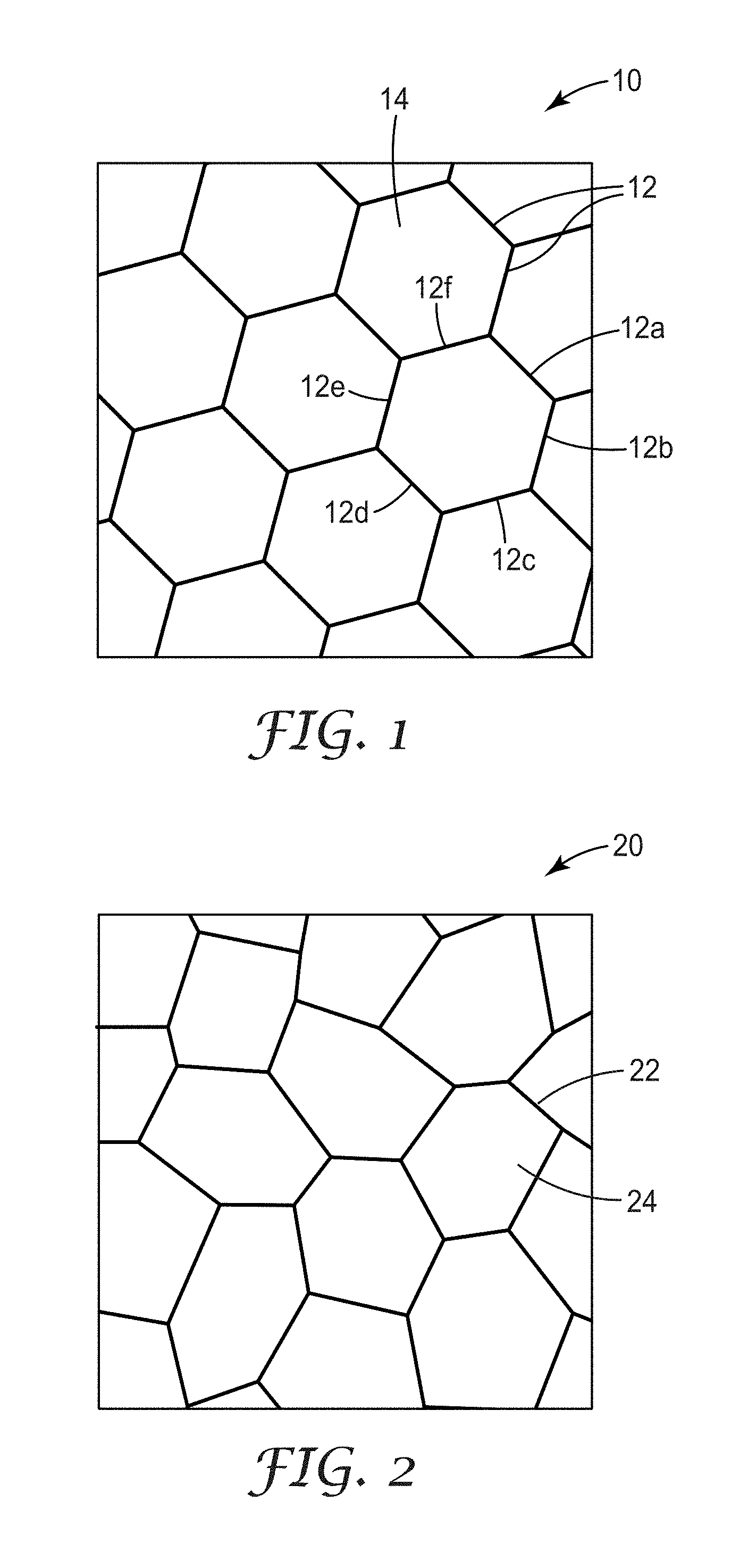
The use of metal-based meshes for applications where electrical conductance and light transmission are required is well known. These applications include shielding against electromagnetic interference in displays. “In the industry, mesh is usually understood as a pattern geometry with connected traces separated by an open area.
It has been noted in the present work that certain mesh designs can produce undesirable visual effects when integrated into displays and viewed in reflected collimated lighting (such as direct sunlight). Examples of undesirable visual effects are, for example, a starburst-like pattern in reflected light, and bands (similar to rainbows) of colored reflected lights caused by interference with light. These are visible when a mesh with linear traces, and repeating cell geometries, is placed on a substrate that has not been modified, such as plastic film or a glass. Meshes with linear traces can be illustrated by hexagonal or square cells. Sparkle can appear on meshes with linear traces.
Some skilled in this art have tried to reduce the appearance of micropatterns overlaid on mesh by using wavy lines in the production of a display such as a touchscreen display. PCT International Publication Number. “WO 2010/099132A2 describes articles such as antennas or electromagnetic interference shields with a transparent light substrate, and two conductive meshes each having linear trace, wherein the first mesh is arranged over a second mesh to minimize the visibility of the traces.
Others have tried to use ambient-light-reducing members, such as optical interference members. PCT International Publication Number. See PCT International Publication No.
The meshes are integrated into displays and can be viewed in reflected or collimated light. This is especially true in direct sunlight.
The present disclosure discloses articles that use substrates with nanostructured surfaces in combination designs of conductor patterns. The combination, when integrated into a device or display, reduces undesirable visual effects such as starbursts, sparkles, halo, and rainbows, which occur under light. This includes but is not limited to collimated, or nearly collimated, light such as sunlight.
The surface of useful substrates is nanostructured. This can be achieved by a variety of methods. The methods include reactive-ion etching of a major first surface of the surface or formation of a structured particle coating on the major surface. “Usable conductor micropatterns include those with linear and non-linear trace designs, those without repeating cells, those where the cells do not form an array, or those which have a uniform distribution in the orientation of the traces.
The present disclosure, in one aspect, provides an article that comprises: (a), a substrate with a first nanostructured, antireflective surface exposed to air, (b), a metallic conductor on the first side of the substrate. Each cell of the conductor has an open-area fraction greater than 80%, a uniform distribution trace orientation and the traces have a specular reflectionance of less than 50% when viewed from an orthogonal direction to the first surface.
The present disclosure also provides an article that consists of a transparent substrate with a first surface nanostructured and a metallic conducting disposed thereon, wherein said first surface nanostructured comprises nanofeatures with a height between 50 and 750 nanometers; a width between 15 and 200 nanometers; and a lateral space from 5 to 500 micrometers. Furthermore, the conductor’s average thickness is greater than 50 nanometers.
The present disclosure also provides a method for making a micropattern that includes the following steps: (a), providing a substrate with a first and opposing second surfaces; (b), modifying the first of these surfaces to include nanofeatures of a height of 50 to 750 micrometers and a width of 15 to 200 micrometers and a lateral space of 5 to 500 micrometers. (c) depositing metallic conductor onto the first of these surfaces including the nanofeatures. (d)


The present invention also provides an article that comprises a transparent substrate with a first microstructured layer and a metallic conductor disposed thereon. Wherein the first microstructured layer comprises nanofeatures of sizes ranging from 75 to 250 micrometers in height, width, and spacing; the conductor’s average thickness is greater than 50 micrometers.
Unless otherwise specified, all numbers used to express feature sizes, quantities and physical properties in the specification and claim are to be understood in all cases as being modified by the term “about”. The numerical parameters in the specification and claims attached are approximate values that may vary depending on the desired properties that those in the art seek to obtain using the teachings provided herein.
The recitation by endpoints of numerical ranges includes any number within the range (e.g. 1 to 5, includes 1, 1.5, 2, 2.5, 3, 3.80 and 4, 5), and also includes any range within it.
As used herein ?micropattern? “As used herein, “micropattern” refers to an array of dots, lines, filled shapes or combinations thereof. Each element has a specific dimension (e.g. The trace width should not exceed 1 mm. In preferred embodiments the micropattern consists of a mesh of traces that define a number of cells. Each trace has a minimum width of 0.5 microns, and is typically not greater than 20 microns. The micropattern feature dimensions can vary depending on which micropattern is selected. In certain preferred embodiments, micropattern features (e.g. In some preferred embodiments, the micropattern feature dimension (e.g. From 1 to 3 micrometers. In the present disclosure, both linear and non-linear traces can be useful.
As used in this document, “visible light transparency” refers to the level of transmission of an unpatterned substrate or article comprising a micropatterned substrate that is at least 60% transmissive for at least one polarization state of visible light. The term “visible light transparent” refers to a level of transmission that is at least 60% transmissive in at least one polarization of visible light. The term visible light transparency is used to describe an article which transmits at least 60% of incident light and includes microscopic features, such as dots, squares or traces of minimum dimensions. The width of the feature can be between 0.5-10 micrometers or 0.5-5 micrometers. The term “visible” is used to describe the light that can be seen. The term ‘transparent light visible’ is used in conjunction with the term?visible? The term “light” is modified to specify the wavelength range of light for which the substrate or micropatterned article is transparent. “Specify the wavelength range for which the micropatterned substrate or article is transparent.
As used in this document, “open area fraction” is the percentage of a micropattern or region that is not shadowed by a conductor. The open area (or percentage of open space) of a micropattern or region is the portion of the micropattern or region that is not shaded by a conductor. The open area equals one less the area fraction shadowed by the micropattern. It can be expressed interchangeably as a decimal, or percentage. The area fraction shadowed by a conductor pattern is interchangeable with its density (e.g. density of traces defining a mesh). In the present disclosure, values of open area fraction that are useful as examples include those greater or equal to 50%, greater or equal to 75%, 90%, 95%, 96%, 97%, 98%, 99%, and 99.25-99.75%. Other values include 99.8% 99.85% 99.9%, and even 99.95. In some embodiments the open area of the region of the micropattern conductor (e.g. a transparent conductive region visible to light) is between 80%-99.5%.
As used herein, ?trace? The geometric element that is created by the intersection between two planes, or the intersection between a plane with a non-planar plane. Here, the geometric element that is given by an intersection of two planes (or as a trace) is described as linear. Herein, the geometric element resulting from an intersection between a plane with a nonplanar surface (or as a trace) is described as nonlinear. A linear trace is a straight line with zero curvature or, to put it another way, an infinite radius of curve. Non-linear traces have a curvature that is not zero, or to put it another way they have a curvature with a finite radius. As is well known in analytical geometry, the radius or curvature of a curve can be calculated for any point on a line. As is known in analytical geometry, it is possible to construct a normal at any point on a non-linear or linear trace.
As used herein, ?antireflective? Refers to a surface’s or coating’s ability to reduce Fresnel reflection at an interface between a medium and the material to which it is exposed and increase light transmission. Surfaces that reduce reflection at the interface between a material and air are antireflective surfaces when exposed to the air. “In the absence of a surface or coating that reduces reflection, Fresnel reflectance is determined by the difference in refractive indexes between the material and surrounding medium. This is well-known to the art.
As used in this document, “nanostructured” refers to a surface that includes topography in the form of nanofeatures. The nanofeatures are made up of material which defines the surface. “A surface with topography that is in the form nanofeatures. The nanofeatures are made up of material that defines the surface. At least one of their height or width is less than a micron.
Micropattern Designs


The present disclosure can make use of a variety of geometries and designs. There are four classes of mesh pattern design: (A), those with repeating cells geometry (B), those without repeating cells geometry (C), those with centroids that don’t lie on a repeated array (D), and those where the traces are distributed uniformly. These classes do not have to be mutually exclusive. In each of these classes the traces may be linear (i.e. having a finite radius curvature) or non-linear. The mesh micropatterns are not restricted in terms of the size of the cells or the width of the traces. In some embodiments the traces are in a range from 0.1 micrometers to 20 micrometers. Other embodiments have traces in a range between 0.5 and 10 micrometers. In some embodiments the open area (e.g. a visible-light transparent conductive region), is between 80% to 99.5%.


Click here to view the patent on Google Patents.


